Strategic Professional Development Program for Young Researchers
Top Runner Development Program Engaging Universities,
National Labs, and Companies
Strategic Professional Development Program for Young Researchers
Top Runner Development Program Engaging Universities,
National Labs, and Companies
Associate Professor
Institute of Pure and Applied Sciences
University of Tsukuba
2012/ 3 Ph.D, Electronics Science and Engineering, Kyoto University, Kyoto, Japan
2012/4~2014/3 JSPS Overseas Research Fellow, (UCSB, CA, US.)
2014/4~2015/3 Research associate, Basic Research Labolatory, NTT
2015/4~2018/3 Assistant Professor (International tenure track), the Univ. of Tsukuba
(2015/4~2016/3 Visiting researcher, EPFL, Switzerland)
(2016/4~2018/3 Visiting researcher, MIT, US)
2018/4~present Assistant Professor (tenure), the Univ. of Tsukuba
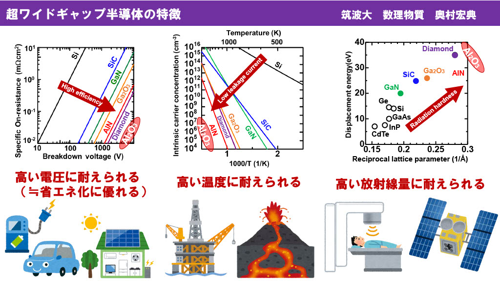
We have worked on the device fabrication and crystal growth for power devices and ultraviolet LED. Particularly, our group has focused on Gallium-oxide (β-Ga2O3) and Aluminum-nitride (AlN) devices. These materials would significantly contribute to the saving energy. In 2018, we achieved the first demonstration of AlN-channel transistors. Recently, we firstly reported the room-temperature electrically conductive sapphire (α-Al2O3). Sapphire-based materials would contribute to the high-power, high-temperature, and high-radiation-tolerance devices at low cost.
Our research goal is to connect everything in the earth, in space, and in the biological body through semiconductor devices. By making the most of semiconductor properties, we would like to discover new possibilities over the wall of my research field.
OKUMURA, Hironori, TRiSTAR Fellow (1st-term)
In Preparation.